 | –≠–ª–µ–∫—Ç—Ä–æ–Ω–Ω—ã–π –∫–æ–º–ø–æ–Ω–µ–Ω—Ç: STW5093 | –°–∫–∞—á–∞—Ç—å:  PDF PDF  ZIP ZIP |
1/34
STw5093
March 2004
FEATURES:
Complete CODEC and FILTER system including:
14 BIT LINEAR ANALOG TO DIGITAL AND
DIGITAL TO ANALOG CONVERTERS.
8 BIT COMPANDED ANALOG TO DIGITAL
AND DIGITAL TO ANALOG CONVERTERS A-
LAW OR
µ-LAW.
TRANSMIT AND RECEIVE BAND-PASS
FILTERS
ACTIVE ANTIALIAS NOISE FILTER.
Phone Features:
ONE MICROPHONE BIASING OUTPUT
REMOTE CONTROL (REMOCON) FUNCTION
THREE SWITCHABLE MICROPHONE
AMPLIFIER INPUTS. GAIN
PROGRAMMABLE:0 . . 42.5 dB AMPLIFIER,
1.5 dB STEPS (+ MUTE).
EARPIECE AUDIO OUTPUT. ATTENUATION
PROGRAMMABLE: 0 . . 30 dB, 2 dB STEPS.
EXTERNAL AUDIO OUTPUT. ATTENUATION
PROGRAMMABLE: 0 . . 30 dB, 2 dB STEPS.
DRIVING CAPABILITY: 140mW OVER 8
TRANSIENT SUPRESSION SIGNAL DURING
POWER ON AND DURING AMPLIFIER
SWITCHING.
INTERNAL PROGRAMMABLE SIDETONE
CIRCUIT. ATTENUATION PROGRAMMABLE:
16 dB RANGE, 1 dB STEP.
INTERNAL RING, TONE AND DTMF
GENERATOR, SINEWAVE OR
SQUAREWAVE WAVEFORMS.
ATTENUATION PROGRAMMABLE: 27dB
RANGE, 3dB STEP. THREE FREQUENCY
RANGES:
a) 3.9Hz . . . . 996Hz, 3.9Hz STEP
b) 7.8Hz . . . . 1992Hz, 7.8Hz STEP
c) 15.6Hz . . . . 3984Hz, 15.6Hz STEP
PROGRAMMABLE PULSE WIDTH
MODULATED BUZZER DRIVER OUTPUT.
General Features:
SINGLE 2.7V to 3.3V SUPPLY
EXTENDED TEMPERATURE RANGE
OPERATION (*) -40∞C to 85∞C.
1.0
µW STANDBY POWER (TYP. AT 2.7V).
13mW OPERATING POWER (TYP. AT 2.7V).
1.8V TO 3.3V CMOS COMPATIBLE DIGITAL
INTERFACES.
PROGRAMMABLE PCM AND CONTROL
INTERFACE MICROWIRE COMPATIBLE.
APPLICATIONS:
GSM/DCS1800/PCS1900/JDC DIGITAL
CELLULAR TELEPHONES.
CDMA CELLULAR TELEPHONES.
DECT/CT2/PHS DIGITAL CORDLESS
TELEPHONES.
BATTERY OPERATED AUDIO FRONT-ENDS
FOR DSPs.
(*) Functionality guaranteed in the range - 40∞C to +85∞C; Timing
and Electrical Specifications are guaranteed in the range - 30∞C
to +85∞C.
GENERAL DESCRIPTION
STw5093 is a high performance low power combined
PCM CODEC/FILTER device tailored to implement the
audio front-end functions required by low voltage/low
power consumption digital cellular terminals. STw5093
offers a number of programmable functions accessed
through a serial control channel that easily interfaces to
any classical microcontroller. The PCM interface sup-
ports both non-delayed (normal and reverse) and de-
layed frame synchronization modes.
STw5093 can be configurated either as a 14-bit lin-
ear or as an 8-bit companded PCM coder.
Additionally to the CODEC/FILTER function, STw5093
includes a Tone/Ring/DTMF generator, a sidetone gen-
eration, and a buzzer driver output.STw5093 fulfills and
exceeds D3/D4 and CCITT recommendations and ETSI
requirements for digital handset terminals.
Main applications include digital mobile phones, as
cellular and cordless phones, or any battery powered
equipment that requires audio codecs operating at
low single supply voltages.
TSSOP30
ORDERING NUMBER: STw5093
2.7V SUPPLY 14-BIT LINEAR CODEC WITH
HIGH-PERFORMANCE AUDIO FRONT-END
STw5093
2/34
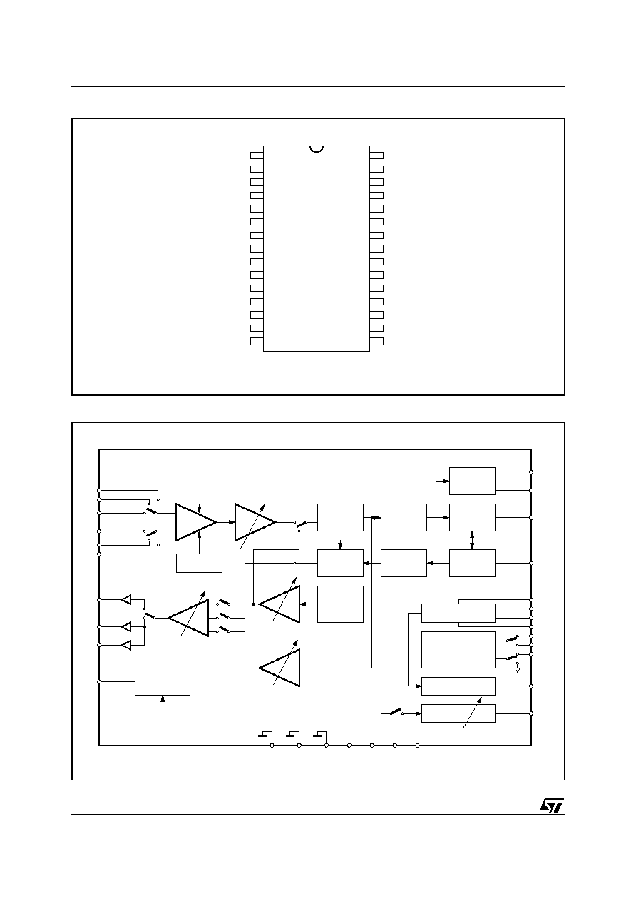
PIN CONNECTIONS (Top view)
BLOCK DIAGRAM
VCC
REMOUT
REMIN
MIC3+
VCCP
VLr+
VLr-
GNDP
LO
VFr
DX
DR
FS
MCLK
1
3
2
4
13
14
15
28
27
18
17
16
29
30
D98TL399
GNDA
MIC2-
MIC2+
BZ
CS-
CCLK
10
11
12
21
20
19
MIC1-
CI
9
22
MIC3-
MIC1+
VCCA
AUXCLK
GND
VCCIO
5
7
8
26
24
23
MBIAS
CO
6
25
VS & TE
MIC PREAMP
0/20dB
+ MUTE
MIC AMP
0 -> 22.5
1.5dB STEP
DE
(A)
(B)
TX FILTER
PCM ADC
RX FILTER
PCM DAC
TRANSMIT
REGISTER
REMOCON
REN,RLM,ROI,RDL
RECEIVE
REGISTER
6dB
-1
1
12dB
OE
TONE, RING
& DTMF
GENER.
& FILTER
EARA OUTPUT
0 -> -30dB,
2dB STEP
EXTA OUTPUT
RTE
SE
SI
TONE AMP
0 -> -27dB
3dB STEP
SIDETONE AMP
-12.5 -> -27.5dB
1dB STEP
CONTROL INTERFACE
µ-WIRE
CLOCK GENERATOR
& SYNCHRONIZER
INTERFACE LATCH
BUZZER
DRIVER
BE
EN
GNDP
GNDA
GND
VCCA
VCC
VCCP
LEVEL ADJUST
(PWM)
MIC3-
MIC2-
MIC1-
MIC2+
MIC1+
MIC3+
VFr
VLr-
VLr+
DX
REMOUT
REMIN
CO
DR
CI
CS-
CCLK
FS
MCLK
LO
BZ
D98TL408
PG
MICROPHONE
BIAS
MBIAS
HPB
VCCIO
AUX CLK
SLC
MB
3/34
STW5093
PIN FUNCTION
N∞
Pin
Description
1
V
CC
Power supply input for the digital section.
2
REMOUT Remocon function digital output.
3
REMIN
Remocon function input. An high level at this pin is detected as a non pressed key, while a low
level is detected as a pressed key.
4
MIC3+
Third positive high impedance input to transmit preamplifier for microphone connection.
5
MIC3-
Third negative high impedance input to transmit preamplifier for microphone connection.
6
MBIAS
Microphone Biasing Switch.
7
V
CCA
Power supply input for the analog section. V
CC
and V
CCA
can be directly connected together for
low cost applications (see STw5093 Power Supply Notes).
8
MIC1+
Positive high impedance input to transmit pre-amplifier for microphone connection.
9
MIC1-
Negative high impedance input to transmit pre-amplifier for microphone connection.
10
GNDA
Analog Ground: All analog signals are referenced to this pin. GND and GNDA can be connected
together for low cost applications (see STw5093 Power Supply Notes).
11
MIC2+
Second Positive high impedance input to transmit pre-amplifier for microphone connection.
12
MIC2-
Second negative high impedance input to transmit pre-amplifier for microphone connection.
13
V
CCP
Power supply input for the V
Fr
and V
Lr
drivers. V
CCP
and V
CCA
must be connected together.
14,15
V
Lr-
,
V
Lr+
Receive analog extra amplifier complementary outputs. These outputs can drive directly
earpiece transductor of 8
or 50nF. The signal at these outputs can be the sum of:
- Receive Speech signal from DR,
- Internal Tone generator,
- Sidetone signal.
16
GNDP
Power ground. V
Fr
and V
Lr
drivers are referenced to this pin. GNDP and GNDA must be
connected together.
17
V
Fr
Receive analog earpiece amplifier output. This output can drive directly earpiece transductor of
30
or 50nF. The signal at this output can be the sum of:
- Receive Speech signal from D
R
,
- Internal Tone Generator,
- Sidetone signal.
18
LO
A logic 1 written into DO (CR1) appears at LO pin as a logic 0
A logic 0 written into DO (CR1) appears at LO pin as a logic 1.
19
BZ
Pulse width modulated buzzer driver output.
20
CCLK
Control Clock input: This clock shifts serial control information into CI and out from CO when the
CS- input is low, depending on the current instruction. CCLK may be asynchronous with the
other system clocks.
21
CS-
Chip Select input: When this pin is low, control information is written into and out from the
STw5093 via CI and CO pins.
22
CI
Control data Input: Serial Control information is shifted into the STw5093 on this pin when CS- is
low on the rising edges of CCLK.
23
AUXCLK Auxiliary Clock Input. Values must be 512 kHz, 1.536 MHz, 2.048 MHz or 2.56 MHz selected by
means of Control Register CR0. AUXCLK is not used to shift in and out data
STw5093
4/34
24
VCCIO
Power supply Input for the Digital I/O's.
25
CO
Control data Output: Serial control/status information is shifted out from the STw5093 on this pin
when CS- is low on the falling edges of CCLK.
26
GND
Ground: All digital signals are referenced to this pin.
27
D
X
Transmit Data ouput: Data is shifted out on this pin during the assigned transmit time slots.
Elsewhere DX output is in the high impedance state. In delayed and non-delayed normal frame
synchr. modes, voice data byte is shifted out from TRISTATE output DX at the MCLK on the
rising edge of MCLK, while in non-delayed reverse frame synchr mode voice data byte is shifted
out on the falling edge of MCLK.
28
D
R
Receive data input: Data is shifted in during the assigned Received time slots In delayed and
non-delayed normal frame synchr. modes voice data byte is shifted in at the MCLK frequency on
the falling edges of MCLK, while in non-delayed reverse frame synchr. mode voice data byte is
shifted in at the MCLK frequency on the rising edges of MCLK.
29
FS
Frame Sync input: This signal is a 8kHz clock which defines the start of the transmit and receive
frames. Any of three formats may be used for this signal: non delayed normal mode, delayed
mode, and non delayed reverse mode.
30
MCLK
Master Clock Input: This signal is used by the switched capacitor filters and the encoder/decoder
sequencing logic. Values must be 512 kHz, 1.536 MHz, 2.048 MHz or 2.56 MHz selected by
means of Control Register CR0. MCLK is used also to shift-in and out data.
N∞
Pin
Description
PIN FUNCTION (continued)

5/34
STW5093
1.0 FUNCTIONAL DESCRIPTION
1.1 DEVICE OPERATION
1.1.1 Power on initialization:
When power is first applied, power on reset circuitry initializes STw5093 and puts it into the power down state.
Gain Control Registers for the various programmable gain amplifiers and programmable switches are initialized
as indicated in the Control Register description section. All CODEC functions are disabled.
The desired selection for all programmable functions may be intialized prior to a power up command using the
MICROWIRE control channel.
Note: after register programming, a subsequent activation of the internal Power on Reset can be detected by
programming to 1 the DO bit in the CR1 register; this sets to the logic level 0 the LO output. If an internal Power
on Reset occurs, LO automatically switches to logic level 1.
1.1.2 Power up/down control:
Following power-on initialization, power up and power down control may be accomplished by writing any of the
control instructions listed in Table 1 into STw5093 with "P" bit set to 0 for power up or 1 for power down.
Normally, it is recommended that all programmable functions be initially programmed while the device is pow-
ered down. Power state control can then be included with the last programming instruction or in a separate sin-
gle byte instruction.
Any of the programmable registers may also be modified while STw5093 is powered up or down by setting "P"
bit as indicated. When power up or down control is entered as a single byte instruction, bit 1 must be set to a 0.
When a power up command is given, all de-activated circuits are activated, but output DX will remain in the high
impedance state until the second Fs pulse after power up.
1.1.3 Power down state:
Following a period of activity, power down state may be reentered by writing a power down instruction.
Control Registers remain in their current state and can be changed by MICROWIRE control interface.
In addition to the power down instruction, detection of loss MCLK (no transition detected) automatically enters
the device in "reset" power down state with DX output in the high impedance state.
1.1.4 Transmit section:
Transmit analog interface is designed in two stages to enable gains up to 42.5 dB to be realized. Stage 1 is a
low noise differential amplifier providing a selectable 0 or 20 dB gain via bit 1 (PG) of register CR4. A microphone
may be capacitevely connected to MIC1+, MIC1- inputs, while the MIC2+ MIC2ƒ and MIC3+ MIC3- inputs may
be used to capacitively connect a second microphone or a third microphone respectively or an auxiliary audio
circuit. MIC1 or MIC2 or MC3 or transmit mute is selected with bits 6 and 7 of register CR4.
In the mute case, the analog transmit signal is grounded and the sidetone path is also disabled. Following the
first stage is a programmable gain amplifier which provides from 0 to 22.5 dB of additional gain in 1.5dB step.
The total transmit gain should be adjusted so that, at reference point A, see Block Diagram description, the in-
ternal 0 dBm0 voltage is 0.49 Vrms (overload level is 0.7 Vrms). Second stage amplifier gain can be pro-
grammed with bits 4 to 7 of CR5.
An active RC prefilter then precedes the 8th order band pass switched capacitor filter. A/D converter can be
either a 14-bit linear (bit CM = 0 in register CR0) or can have a compressing characteristics (bit CM = 1 in reg-
ister CR0) according to CCITT A or MU255 coding laws. A precision on chip voltage reference ensures accurate
and highly stable transmission levels.
Any offset voltage arising in the gain-set amplifier, the filters or the comparator is cancelled by an internal au-
tozero circuit.
Each encode cycle begins immediatly at the beginning of the selected Transmit time slot. The total signal delay
referenced to the start of the time slot is approximatively 195
µs (due to the transmit filter) plus 125 µs (due to
encoding delay), which totals 320
µs. Voice data is shifted out on DX during the selected time slot on the trans-